PCBs are in nearly every technological device we use today. Their primary functions are: 1. To electrically connect electronic components and 2. To provide mechanical support (e.i. the electronic components are permanently soldered to the board). PCBs are built in layers similarly to a lasagna. These layers are made of different materials in order to provide structure, durability, conductivity, and organization to the material.
Printed Circuit Boards typically include mechanical layers, solder mask layers, silkscreen layers, solder paste layers and one or more copper layers depending on the complexity of the boards.
The outer layer contain the boundaries (shape and physical dimensions) of the PCB. Additional mechanical layers may contain tooling specification and other mechanical information.
The copper layers contain the routing layers as well as the ground and power planes.
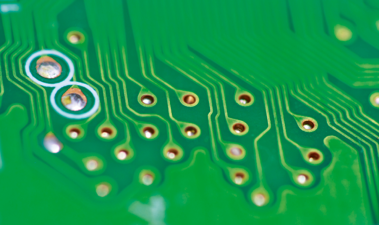
The solder mask is a solder resist coat that is usually applied to the outer layers of the PCB for protection against oxidation and to prevent solder bridges from forming between closely spaced solder pads. Solder mask is usually green but is also available in many colors.
The silkscreen layers contains the reference designators, among other things, for the electronic components located on the top and bottom sides of the board. The text is usually printed with a permanent non-conductive ink. Silkscreen is usually white but is also available in other colors.
The solder paste layers contain the location, the size and the shape of the SMD pads on the board. This information is then used to make the apertures in the SMT stencil.
Reasons For Using Multiple Layers In Printed Circuit Boards.
Miniaturization
Multilayer PCBs enable designers to reduce the board size by adding layers. This is very important as miniaturization of electronic products continue to drive the industry.
Reduced complexity
Multiple layers make PCB routing easy because copper traces in one layer can connect to traces in other layers to complete the path.
Supply and ground isolation
Multi-layer PCBs (4 or more layers) have their own supply and ground layers. This provides isolation between supply and ground pins preventing short circuit.
Simplify Construction & Reduce Weight
Eliminate or reduce the need of connectors for multiple separate PCBs.
Higher density of assembly
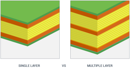
Single Layer Versus Multiple Layer Printed Circuit Boards.
Single Layer PCBs have the electronic components on one side of the board and the conductor pattern on the other side. Multilayer PCBs can have the electronic components on the top side, the bottom side or both sides of boards and have one or more conductor patterns.
Single-layer or single-sided PCBs are typically used in simple electronics. They are cheap to manufacture and are often used in applications that demand high volumes such as calculators, radios, and printers.
Double-layer boards are necessary for moderately advanced technology including HVAC systems, power supplies, LED lighting, and automotive dashboard lighting.
Multi-layered boards delve into the territory of complex data storage, GPS technology, medical equipment, and satellites.