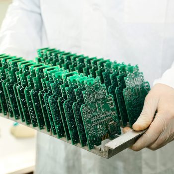
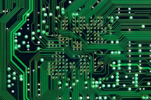
 While prototype circuit boards are used in everything from cell phones to computer monitors, to light switches and televisions, there is a belief that PCB fabrication is standard and straightforward. In fact, this is untrue, as the PCB assembly process is just as versatile as the uses for the boards themselves. Before we break down the materials used in PCB fabrication, it’s important to know these simple things about prototype PCBs.
- There are three major ways to construct a circuit board, single-sided, double-sided, and multi-layered.
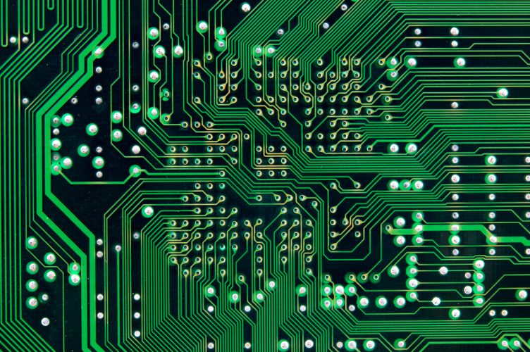
- The most simple printed circuit boards contains copper tracks on only one of their surfaces; this is known as a 1 layer PCB.
- Generally, a two to four layer board will not have drill holes less than 10 mils in diameter, and it will have a five mil minimum for air gaps and trace widths. The typical size should be 0.062 inches, have standard FR-4, and weigh 1 oz.
Manufacturing techniques:
- Photoworks: some companies choose to use this method to develop the PCB layout according to the preferences of the customer.
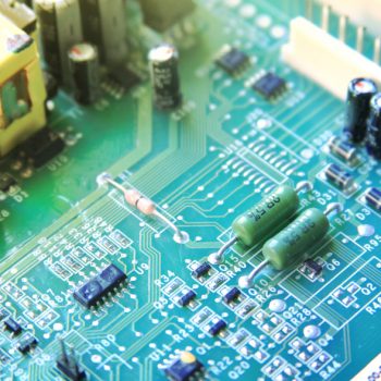
- Material preparation: typically, the material of choice is copper. In this step, the copper plates and a backup board are cut down to size.
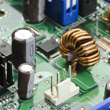
- Drilling: reference and tooling holes are drilled. The engineer may choose to practice through-hole drilling or surface mount technology.
- Plating and coating: engineers will plate the boards with solder, tin, or gold over the nickel surface so the underlying copper does not etch away. For those aspects of the board that cannot be touched by the solder, there is a special solder resist application the engineers can use to protect it.
- Legend printing: a legend is printed on both sides of the PCB and contains component designators, switch settings, and test points. The goal of the legend is to help the engineer assemble the PCB.
There are three methods to legend printing:- Silk-screen printing
- Liquid photo imaging
- Ink jet imaging
- Bare-board test: this tests for any missing connections on the board, or shorts, which are incorrect connections between two points that should be disconnected.
Have any questions? Head over to the PCB fabrication experts at PCB Unlimited for the PCB solutions you need.