Simply give us a call or send us an email. We are here to help.
Phone number: (800) 348-9250
Email: support@pcbunlimited.com
An HDI PCB has a higher wiring density than a traditional PCB. In other words, an HDI PCB’s electric interconnections (its circuits or wiring) require less space than an equivalent number of circuits in a traditional PCB. This permits a more condensed layout of components which allows simpler and shorter traces between them. “Traces” are the tiny, flat networks of copper lines imprinted on a board that transmit electrical signals from one component on the board to another; that is, traces are how a PCB’s components are interconnected.
HDI PCBs are valued because that they feature fewer vias (electrical connections between different layers of a PCB), pads (the metal on a board to which components are soldered), traces, and gaps (the clearance needed between conductors to avoid electrical interference) than a traditional PCB with the same number of interconnections. As a result, HDI printed circuit boards weigh less, have lower material costs, and allow the use of smaller components than traditional PCBs. The use of smaller components permits HDI PCBs to outperform traditional PCBs in functionality, reliability, and energy efficiency. HDI PCBs can serve many applications that traditional PCBs cannot.
HDI PCBs are designed utilizing laser drilled microvias, blind and buried vias, very fine traces, and tiny gaps. A “via” is a copper cylinder placed in holes drilled in the layers of a board that permit electrical signals to transit the layers. Vias are constructed using the technique of sequential lamination. Different types of HDI printed circuit boards use different types and combinations of vias.
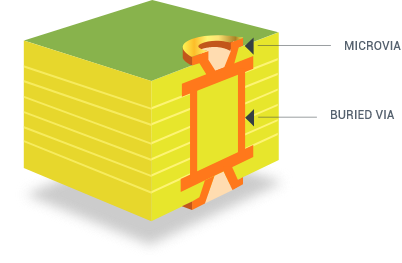
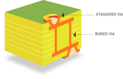
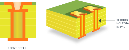
As described above, vias are the conductive holes that connect and allow electrical (or thermal) signals to be transmitted through the multiple layers of an HDI PCB. Vias have different names depending on their position and their construction:
This design uses microvias on the external layers of a board which are connected by a buried via through the interior layers of the board. The buried microvias are filled with copper.
In this design, the external layer microvias are offset from one another.
This design utilizes blind microvias of different diameters. It is not necessary to fill the first level of the blind holes with copper.

These vias are used to assemble components with very fine pitch such as Blind Grid Arrays (BGAs) or Surface Mount Devices (SMDs)) onto the same drilled pads. The buried hole is filled with epoxy resins or copper, then capped with copper.
The Institute for Printed Circuits (IPC) provides six design structures for HDI printed circuit boards. These designs are defined by the IPC-2226 standard. Every structure can be represented by the notation i+[C]+i, with i indicating the number of layers on each side of the “core”: which is represented as [C]. The core of a PCB is the rigid base material onto which copper traces are imprinted. Below are the three most commonly used structures in the manufacture of HDI printed circuit boards.
Include 1 layer of microvias on one or both sides of the core as well as through vias.
![TYPE 1 STRUCTURES (1 [C] 0 OR 1 [C] 1)](/assets/pu/home/hdi-pcbs/structures-1-02ca5de663138bc181ba829eff996c0b0aa55d0b5619eebbba045a7d869eddfd.png)
Applications: Cell phone, MP3 Player, GPS, Memory Card.
Include 1 layer of microvias on one or both sides of the core combined with through vias and blind/buried vias.
![TYPE 2 STRUCTURES (1 [C] 0 OR 1 [C] 1)](/assets/pu/home/hdi-pcbs/structures-2-e23ba94caedb085d9c00780f8586a3a1590694e8ebaec8f8885d9ec92a67624a.png)
Include 2 layers of microvias on one or both sides of the core together with through vias and blind/buried vias.
![TYPE 3 STRUCTURES (≥ 2 [C] ≥0)](/assets/pu/home/hdi-pcbs/structures-3-4406b83a34a8125954bcf52063796149fc0080e6ae61ba2ade45ede833b8ff71.png)
Applications: Cell phone, PDA, Game Consoles, Portable Video Recording devices.
Signal Integrity
Microvias in an HDI board have a significantly improve signal integrity. And, because components are placed closer to one another than in traditional PCBs, more versatile routing is possible, which results in faster signal transmission with greater quality and reduced power consumption. Also, microvias do not introduce parasitic capacitance and inductance problems, thus reducing crosstalk and noise coupling issues.
Cost-effective
Because of the lower number of required layers, smaller dimensions, and the greater number of components, HDI printed circuit boards can function as an all-in-one circuit board rather than requiring multiple boards as with traditional PCBs. When compared to purchasing several traditional PCBs for different programs, an HDI PCB will provide equivalent or superior functionality by means of a smaller board that costs less to produce.
Reliability
Microvias are far more reliable than through-holes due to the usage of a lower aspect ratio (the ratio of the thickness of the board to the diameter of the hole. While HDIs typically use thinner boards than traditional PCBs, the use of stacked vias give the board exceptional strength and resistance power by serviing as a strong shield against adverse environmental conditions. HDI printed circuit boards will perform reliably for much longer than most traditional PCBs.
Faster time to Market
Because of the versatility allowed for component, pad, and trace placement, the reduced number of components required, the usage of vias, and the increased electrical performance, the design and testing process for HDI PCBs is much less time-consuming that for traditional PCBs.
Power/Efficiency
HDI PCBs create a more convenient and effective routing that enables the deployment of several transistors for improved electronics performance while reducing power consumption without sacrificing electrical functionalities.
Reduced Inductance, Capacitance, and Electro-Magnetic Interference
Signal radiation and reflection are major issues with larger vias since they behave as high frequency radiating antennas, especially when a signal resonates in a stub. Microvias are smaller than ordinary vias, hence they have lower emission and absorption cross-sections, and there will be no stubs due to sequential build-up. Because HDI PCBs are built with thinner dielectrics, microvias are closer to ground planes and have better shielding. Finally, because there are no dog-bone pads with traces, filled and capped microvias put directly in component solder lands minimize inductance in the distribution network. All the above elements contribute to decreasing both radio frequency and electro-magnetic interference.
Increased Density of Connections
Microvias-in-pad save space by creating connections inside the pads of surface-mounted technologies (SMTs), in addition to providing more dense connections between layers and with smaller traces. Furthermore, high circuit density boards are required to enable components to be packed into smaller places and allow fine-pitch components to be used. Microvias-in-pad will fit inside the pads of even the finest pitch packages, particularly BGAs, and they will be far more beneficial in breakout channels. Using microvias can enhance escape path width, potentially allowing you to require fewer layers to breakout a BGA, allowing designers to design and install additional components on both sides of the PCB. Other notable improvements in performance include increased thermal dissipation, more stable voltage rail, reduced parasitic loads, and lighter weights than non-HDI printed circuit boards.
HDI PCBs can provide the superior performance and space-saving qualities required by complex electronic devices in today's world of technologies. The HDI PCBs are used in many applications:
Consumer devices
HDI PCBs are employed to achieve sleek designs in modern everyday devices such as smartphones, computers, digital cameras, tablets, touch-screen devices, and home appliances.
Healthcare Industry
Miniature devices have long been in demand in equipment for monitoring, imaging, surgical procedures, laboratory analysis, and other healthcare applications. HDI PCBs have aided in miniaturizing many devices such as cameras, pacemakers, portable X-Rays machines, and external devices such as hearing aids and improving their performance at a lower cost. HDI printed circuit boards have also improved the accuracy of numerous monitoring devices and medical tests.
Automotive
Today's automobiles use large numbers of microprocessors to control the motor, drive, and safety systems, to perform diagnostics, and to perform additional functions like onboard WiFi and GPS, backup sensors, and parking assistance. As a result, vehicle manufacturers are opting for smaller HDI PCBs since their lightweight and small size saves them space and money.
Aerospace
HDI PCBs can endure harsh environmental conditions, making them suitable for use in the design of electronics for missile systems, aviation, and military applications.
Wearables
The tiny circuitries of HCI PCBs renders them highly suitable for wearable gadgets like smartwatches, smart clothing, virtual reality, and more.
Military
HDI PCBs’ robust and compact shape prevents them from breaking down quickly or being damaged by environmental conditions and physical impacts. They are employed in avionics, smart weapons, defense networks, and other forms of communication.
Automation
Industrial automation necessitates extensive computerization. The Internet of Things (IoT) devices that collect data and connect to the internet to communicate with other smart devices, as well as relay information to management and help optimize operations, are now ubiquitous in manufacturing, warehousing, and other industrial settings.


PCB Unlimited is truly the best source for printed circuit boards including HDI PCBs. We offer domestic and offshore PCBs. We have an extensive network of PCB manufacturing partner in Taiwan and China. Each partner has a unique set of manufacturing capabilities. We can make your prototypes or mass produce the boards you need. You will find our pricing highly competitive and our customer service excellent. For a custom quote please email your Gerber files to support@pcbunlimited.com or contact us to discuss your requirements at (800) 348-9250.