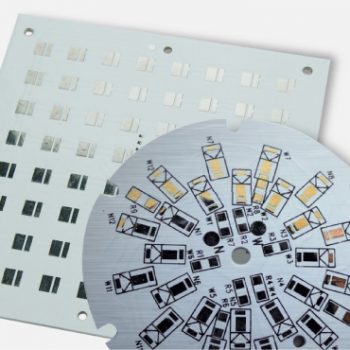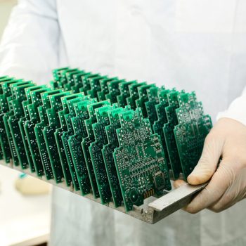
Single-sided, double-sided, and multilayered are the three main types of PCBs (Printed Circuit Boards). There are several individual stages deployed in the course of PCB assembly. All of them need to function as a team to produce an overall integrated process. Every stage needs to flow into the next, and feedback after the final stage is necessary in order to maintain quality. By doing so, any issue is quickly spotted and the necessary adjustments are made. Here is an overview of the PCB assembly process.
1. Solder Paste
Solder paste has to be added in requisite areas before any component is added to the board. Some of these areas include component pads, where solder addition is done using a solder screen. Solder paste is in form of minute solder grains laced with flux. This mixture is added to the appropriate place in a manner that mirrors typical printing processes.
By moving a runner across the screen, solder paste permeates through the screen holes and gets deposited on the PCB board. Note that the solder deposits are only found in the solder pads. This is because the printed circuit board files are used to generate the solder screen. Therefore, the solder screen holes are always in line with the solder pads. For the best PCB fabrication result, the solder amount needs to be monitored so that the correct volume goes into the resulting joints.
2. Pick and Place
In this part of the PCB fabrication and assembly process, the board undergoes a process known as pick and place. A pick and place machine takes the components from the dispenser and puts them in the needed location on the board. Tension from the solder paste helps in keeping all the components in their rightful place on condition that the PCB doesn’t shake. In order to keep components secured on the board, some pick and place machines add glue drops during the PCB fabrication process. To avoid repair complications, degradable glue is the best to use during the soldering process.
3. Soldering
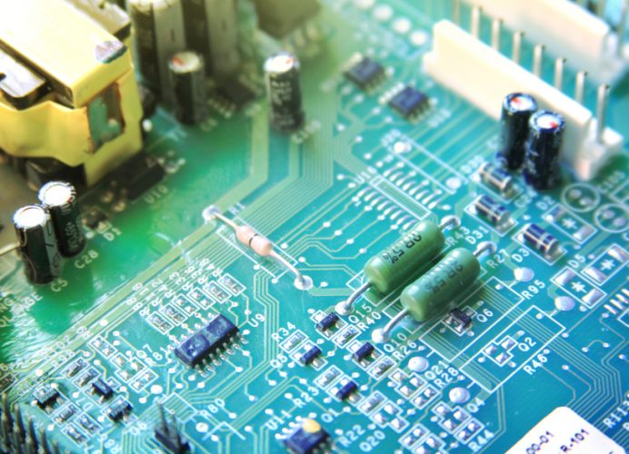
Now that the necessary components are already on the PCB, it is now time to pass the board through a soldering machine. Though not as common nowadays, some PCB fabrication processes involve passing the board through wave soldering machines. Solder paste addition to the board isn’t necessary with wave soldering because the machine has its own solder. In place of wave soldering, most PCB manufacturers prefer using a reflow oven.
4. Inspection
Once the soldering stage is complete, printed circuit boards need to be inspected. When it comes to surface mounts, manual inspection is impossible considering that the board has many components. It would also need a lot of employees to perform manual inspections and this would not make economic sense. Automatic optical inspection, on the other hand, is a much better way of going about this. These machines have what it takes to detect misplaced components, poor joints, and even wrong components.
5. Testing
Electronic products need to be tested before leaving the factory, and PCBs are no exception. Testing helps in knowing whether the printed circuit board is functioning properly. Some of the methods used to test boards after PCB fabrication are:
- A quick visual inspection to ensure all electrical components are in place.
- Analog signature analysis: This involves the use of AC current across two areas of the circuit and electrical components.
- Functional testing: This helps in verifying whether the printed circuit board does what it is intended to do.
- In-circuit testing: This involves checking numerous parameters like frequency and voltage.
6. Feedback
Monitoring the outputs helps in knowing whether the PCB fabrication process is going on well. A good way of achieving this is by investigating all detected failures. The optical inspection stage is the best time to do so because it usually takes place after soldering. Therefore, any defects are quickly identified and corrected before the mass production of boards with the same problem.
Conclusion
There are many uses of a printed circuit board today. From televisions to microwaves and anything in between, PCBs are almost everywhere in the electronic world. With the above information, you now know what PCB fabrication and assembly is all about.