When you chose to invest in your prototype printed circuit boards otherwise known as PCBs, you might wonder how your PCB assembly process is so precise. The PCB manufacturing process has changed greatly over the years, and it’s thanks to new technological innovations that have allowed circuit board manufacturers to innovate accurately and skillfully.
Here’s how prototype PCBs are made with such accuracy.
Front-End Engineering Checks
Before a PCB prototype is built, there are countless aspects that go into planning the final result. First, the PCB manufacturer will look over the board design (Gerber files), and begin preparing the circuit board with a list of step-by-step instructions that are laid out for fabrication. After review, an engineer will then convert these plans into a data format that will help to engineer the PCB. This engineer also will check for any issues with format or clean up.
This data is used to create the final board, which is also given a unique tool number. This number keeps track of the printed circuit boards that go through the building process. Even the smallest of changes to a circuit board revision will result in a new tool number, which helps to ensure there is no confusion during the PCB manufacturing and fabrication processes of multiple orders.
Plotting
After the correct files are inspected, and a panel array is chosen for the best fit, photo plotting begins. This is the start of the production process. The photoplotter utilizes a laser to plot the patterns, silk screens, and other primary images that are required on the PCB.
Lamination and Drilling
One of the three primary types of printed circuit boards, multi-layered PCBs, require lamination to fuse the multiple layers together. This is typically done using heat and pressure.
Once the product is laminated, expert drilling systems are programmed to drill holes precisely and accurately into the boards. The drilling program ensures that there is no human error during the PCB manufacturing process.
Copper Deposition and Plating
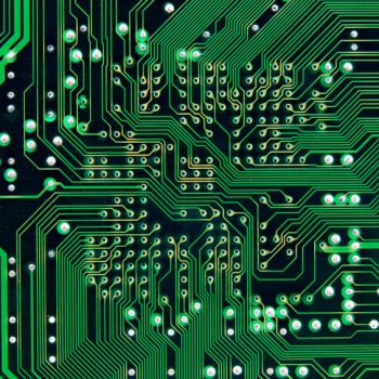
The conductive copper layer, which is deposited through electrolysis, is essential to the functionality of all prototype printed circuit boards. PCBs officially become conductive surfaces after electroplating, which is where the copper is plated via a plating bath. These copper tracks are a type of conductive path that connect two points within the PCB.
After the prototype printed circuit boards are tested for quality assurance, they are then fabricated into cross sections and lastly, inspected for cleanliness.
For more information on PCB manufacturing, contact PCB Unlimited today!