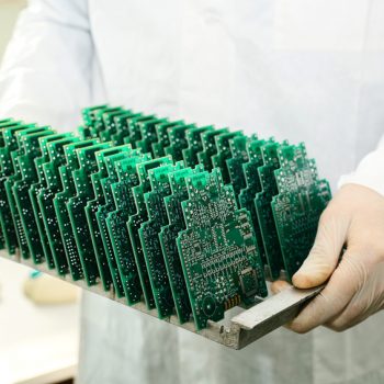
There is a lot that goes into the building of electronics. Not only should an engineer make sure the circuit works properly, the layout of the printed circuit board prototypes is equally as important. The PCB layout is one of the most important factors to make sure an electronic device works, because if not a faulty layout can cause functionality and reliability problems. Here are some PCB layout tips and tricks that will ensure your component works every time.
Sizing the traces
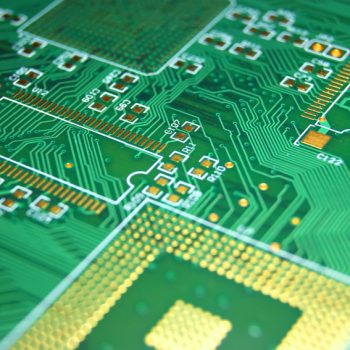
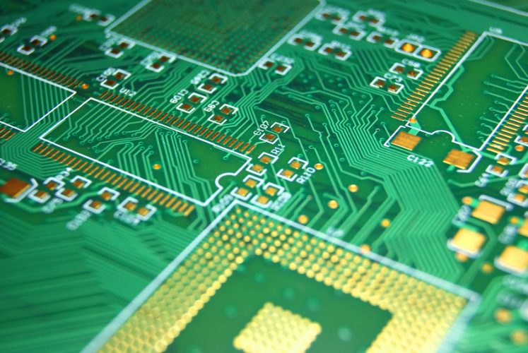
On a prototype PCB, the engineers will use length, thickness, and width to control the resistance of a trace. The resistance is determined by what metal is used, and most engineers tend to use copper in prototype PCBs to make them work efficiently. Simply put, these copper tracks are conductive paths that are used to connect two points within the PCB, and since you cannot change the properties of the copper, an engineer can focus on developing the proper size of the trace for the board in question.
Most engineers use one or two ounces of copper throughout the entire board, but if there are details within the layout such as closely laid pins the thinner the copper should be.
Size of the loops
In general, the loops on your circuit board prototyping should be made as small as possible, especially if they have high frequency. This is because putting loops over a ground plane with a high frequency will reduce inductance, which is crucial for the overall functionality of the board.
Stay away from ground conductors
As a rule of thumb, a ground conductor is not a conductor you should strive for. If you have noisy ground traces, make sure to route them away from signals that must be silent, or else the quality of the currents must be compromised. Ideally, you should place a ground plane directly under the signal and trace it through another layer.
It is no secret that printed circuit board prototypes are quite complex pieces of technology and every detail from the start of their assembly to the finishing touches of their layout. There is so much to incorporate in order to have a working board, so stay tuned for our next post that will go over more tips and tricks for PCB layouts.