Circuit board prototyping is a great way to launch into the field of electronic engineering. However, there are many terms that are crucial to understanding PCB fabrication and assembly, so we have compiled a comprehensive list of commonly used definitions in the world of prototype printed circuit boards.
Activating: The chemical treatment that allows non-conductive laminate to accept electroless deposition. Also known as catalyzing.
Anode: The positive element used in the plating tank, as the power supply is connected to the positive potential. Generally, the anodes are used to supply and accelerate the metal ions on the board towards the circuit that is being plated.
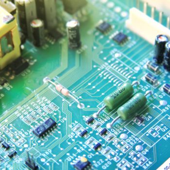
Array: A group of circuits specifically arranged in a pattern.
B-stage Material: Fiberglass sheet cloth material with a layer of resin that is cured to an immediate stage. Also known as pre-preg.
Barrel: The wall that is formed by plating a hole that was drilled.
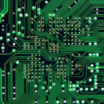
Base Copper: Copper foil in sheet form that is laminated onto one or both sides of the prototype PCBs and used as a conductive path to connect two points in the PCB.
Bed of Nails: A technique of testing prototype PCBs that mounts an array of contact pins configured so as to engage plated thru-holes on the board.
Blind Via Hole: A plated through hole that connects an outer layer on the board to an inner layer, but doesn’t extend fully through all the layers of the base material in the board.
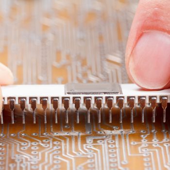
CAD: Computer Aided Design, a software that allows engineers to easily create and design a printed circuit board.
Card-edge connector: A gold-plated connector adhered to the side of the board.
Center to Center Spacing: The nominal distance between the centers of each adjacent feature on the board. This can be on any layer, and is also known as pitch.
Deburring: The process of removing traces of base copper material that remain around the holes after drilling on the board.
Digitizing: A method of converting feature locations on a flat plain to a digital representation in X-Y coordinates.
Edge Bevel: A bevel operation used on edge connectors in order to improve their wear and ease of installation.
Fine Line Design: Printed circuit design that allows two or three traces between adjacent DIP pins. Generally, these lines are about 2mil thick.
Finger: A gold plated terminal of edge-card connector.
Stay tuned for our continuation of this list in part 2!