Before choosing the right prototype PCB technology, it’s important to first understand the PCB-related requirements of the telecommunications and networking industry
| Application Requirements | Electrical, Mechanical or Thermal Requirements | PCB Technology Used |
| High-speed data transmission | Controlled impedance, low signal loss, and minimal crosstalk | Controlled-impedance, low-loss material, HDI, multilayer, and rigid-flex PCBs. |
| High-frequency operation | Low-loss and stable dielectric materials | RF/microwave, ceramic, and low-loss material PCBs |
| Low electromagnetic interference | EMI/EMC control | Controlled-impedance, RF/microwave, HDI, and multilayer PCBs with dedicated ground and power planes for shielding |
| Complex and space-constrained designs | Dense, compact, and flexible layouts. | Multilayer, HDI (high-density interconnect), flex and rigid flex printed circuit boards |
| Prevent service interruption of 24/7, high-power systems | Effective thermal management | Metal core, heavy copper, ceramic and rigid flex (with thermal layers) PCBs |
The selected prototype PCB technology must provide strong signal integrity through controlled impedance, low signal loss, and minimal crosstalk. It should support high-speed, multilayer designs with dedicated power and ground planes for complex routing, provide effective thermal management for 24/7 high-power environments, use stable low-loss materials for high-frequency signals, and include EMI/EMC control to reduce interference and meet regulatory standards.
Commonly Types of PCBs used in Telecommunications and Networking Applications
Multilayer boards support complex designs with high-speed signals. By using multiple signal layers with dedicated power and ground planes, prototype PCBs can maintain controlled impedance, reduce noise and crosstalk, and improve signal integrity for high data speeds. Multilayer designs also improve heat dissipation and help control EMI/EMC.
High-density interconnect (HDI) PCBs enable the use of fine-pitch components, microvias, and compact layouts needed in modern telecommunications and networking equipment.
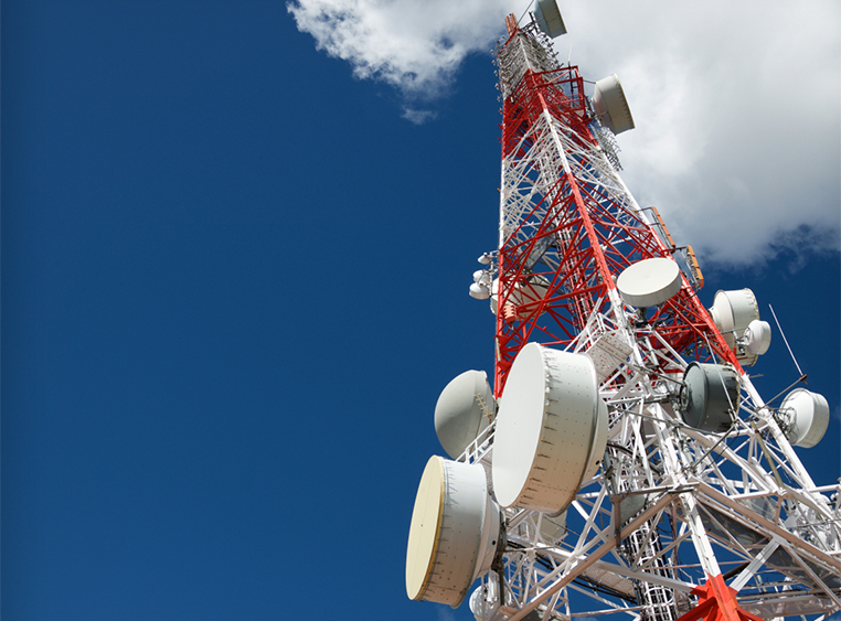
High-frequency / RF PCBs are fabricated with special materials that can transmit high frequency signals above 500MHz with minimal losses. They are commonly used in wireless, 5G, and microwave systems.
Flex and Rigid-flex PCBs are used in telecommunications and networking for their ability to support compact, complex interconnections and perform reliably in small and/or moving spaces. They are also durable and resistant to heat.
Metal core PCBs typically made of aluminum or copper are used to provide signal integrity at high speeds in compact designs by dissipating heat from high-power components. Keeping the temperature low reduces signal distortion and noise that can occur as materials get hot. They also provide mechanical stability and solid ground reference, that helps control impedance and minimize electromagnetic interference.
PCB Design Considerations
Maintaining signal integrity is critical in telecommunications and networking printed circuit board designs. Designers must control impedance, minimize crosstalk and signal loss, manage EMI/EMC, and use multilayer stack-ups with power and ground planes. Heat dissipation and material selection are also essential.
Controlled Impedance works by providing a uniform signal path across the prototype PCB, where high-speed signals can travel smoothly without distortion and with reduce noise, and data errors. This is achieved by managing trace width, trace spacing, copper thickness, dielectric material, and the distance to the reference ground and power planes.
In telecommunications and networking applications, even small impedance variations can cause signal errors, reduced data rates, or produce unreliable communication. Proper impedance control in prototype printed circuit boards helps validate clean, high-speed signal transmission for technologies such as Ethernet, fiber optics, and 5G.”
Signal Loss refers to the reduction in signal strength as it travels along printed circuit board traces. It is caused by factors such as dielectric loss, copper resistance, surface roughness, and impedance mismatches.
In telecommunications and networking applications, where systems operate at high speeds and frequencies, even small losses can reduce signal quality and limit transmission distance. Designers can reduce signal loss by using low-loss materials, controlling impedance, and employing proper grounding and power planes on their prototype printed circuit boards.
Low Crosstalk and Noise refer to unwanted electromagnetic interference between nearby signal traces on a prototype PCB. In telecommunications and networking, too much interference can distort signals, cause data errors, and reduce speed and reliability. Designers limit these problems by spacing traces properly, using solid ground planes, controlling impedance, and carefully designing layer stack-ups.
High-density Multilayer PCBs support compact, complex designs by using fine-pitch components, narrow trace spacing, microvias, and stacked copper layers to separate signal, power, and ground planes. These boards are essential in telecommunications and networking applications because they provide dedicated signal, power, and ground planes that improve signal integrity, reduce noise, and enable complex routing and fine-pitch components to fit into limited space.
Thermal Management (heat control) is very important in telecommunications and networking systems that run all the time at high speeds and power levels. If heat isn’t managed well, it can reduce signal quality and shorten the life of components. Prototype PCB designers control heat by choosing the right materials, optimizing layouts, and using cooling methods to keep boards from overheating.
Fabrication Considerations for Prototype PCBs
Prototype PCBs for telecommunications and networking use advanced manufacturing features. High-speed and high-frequency designs need controlled impedance, tight trace spacing, and well-planned multilayer stack-ups with the right material thickness and copper weight.
PCB fabrication should include solid ground planes, via stitching, and shielding to reduce interference. Surface finishes like ENIG, ENEPIG, and immersion silver help with fine-pitch parts, good soldering, and consistent high-speed performance. Advanced features such as microvias and blind and buried vias support are used to support high-density routing.
For high-power designs, heat control uses copper areas, thermal vias, thicker copper, and metal-core boards to move heat away from components. The PCB fabrication process should also support mass production so designs can move smoothly from prototype to full production.
Material selection
The table below lists stable, low-loss laminate materials designed for high-speed and RF applications.
| PCB Technology | Material Name & Short Description | Typical Devices / Equipment |
| Standard Multilayer PCBs | FR-4 Glass-reinforced epoxy laminate: cost-effective and suitable for moderate-speed digital signals | Ethernet switches, routers, servers, network interface cards |
| High-Speed / Low-Loss Printed Circuit Boards | Low-loss FR-4 (Megtron 6, Isola I-Speed, Nelco): improved dielectric stability and lower signal loss than standard FR-4 | High-speed backplanes, data centers, high-speed networking equipment |
| High-Frequency / RF PCBs | Rogers (RO4000, RO3000 series): low dielectric loss and stable performance at high frequencies | Antennas, RF modules, 5G radios, microwave links, radar systems |
| RF + Digital Hybrid PCBs | Rogers + FR-4 hybrid stack-ups: combines RF performance with lower-cost digital layers | Wireless base stations, telecom transceivers, mixed-signal systems |
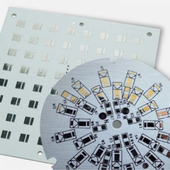
| Metal Core PCBs (MCPCB) | Aluminum or Copper Core: metal base provides excellent heat dissipation | Power amplifiers, LED modules, high-power RF boards |
| HDI (High-Density Interconnect) Printed Circuit Boards | FR-4 or Low-loss HDI materials: supports microvias, fine traces, and compact layouts | Compact networking devices, high-port-count switches, small RF modules |
| Flexible PCBs | Polyimide (PI): thin, flexible, and heat-resistant material | Antennas, wearable telecom devices, internal cable replacement |
| Rigid-Flex PCBs | FR-4 + Polyimide: combines rigid sections with flexible interconnects | Compact telecom equipment, rugged networking hardware |
| Ceramic Printed Circuit Boards | Alumina (Al₂O₃), Aluminum Nitride (AlN): excellent thermal and electrical stability | High-frequency RF modules, microwave components, harsh-environment telecom |
| PTFE-Based PCBs | Teflon-based materials (Rogers RT/duroid): ultra-low loss for very high frequencies | Satellite communications, radar, microwave antennas |
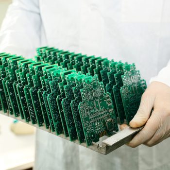
Assembly Considerations for Prototype PCBs
PCB assembly for telecommunications and networking must deliver high-speed performance, reliability, and scalability while protecting signal integrity, managing heat, and allowing a smooth transition from prototype to full production.
Component Placement: Sensitive analog and RF components should be isolated from noisy digital or power circuits.
Controlled impedance and Signal Path: Poor soldering, solder mask misalignment, or wrong component placement can affect impedance and signal quality.
Reflow Profile: Properly set reflow profiles can prevent heat damage and defects that could affect signal quality or reliability.
EMI/EMC: PCB assembly should include proper grounding, shielding, and connector installation.
Thermal Management (heat control): High-power components need strong solder joints, good heat spreading, and secure connection to thermal vias, copper pours, or heat sinks.
Reliability and Durability: Printed circuit board assemblies must have strong solder joints, solid connectors, and resist vibration and temperature changes.”
Prototype PCB assembly should use the same materials and processes as production so they can move to full-scale manufacturing without problems.
Testing Considerations for Prototype PCBs
Testing is a key part of prototyping, and for telecom and networking PCB testing goes beyond basic electrical checks to validate signal quality, thermal performance, EMI/EMC compliance, and long-term reliability in both prototypes and full production. Key considerations include:
Electrical Testing: Use in-circuit or flying probe tests to check all connections and ensure that the prototype PCB is built correctly before functional testing.
Signal Integrity Testing: Verify that high-speed signals can travel correctly without distortion or interference using tools such as TDR, eye diagrams, and network analyzers
Functional Testing: Confirm that the prototype PCB works as expected under real-world conditions, checking speed, response time, and network standards like Ethernet or 5G.
EMI/EMC Testing: Check that the prototype PCB doesn’t cause or get affected by electromagnetic interference and meets industry standards.
Thermal Testing: Check the prototype PCB at extreme temperatures and continuous use to make sure it handles heat well and operates reliably all the time.” Testing methods used in prototyping should be scalable to production.
Conclusion
Prototype PCBs are essential for developing reliable, high-performance telecom and networking equipment, allowing engineers to test and refine designs, check performance, materials, and assembly, and catch potential issues before full production.