CALL US
(800) 348-9250

EMAIL US AT
support@pcbunlimited.com
There are generally two types of technologies used during the PCB Assembly process, through hole (THT) and surface mount (SMT). There is another technology that is becoming common these days that is used when there is a need to mount a single module board on top of another PCB, this technology is called board-to-board soldering. Castellated holes (also referred to as castellations) are becoming more common in printed circuit board fabrication as the demand for circuit board modules increases.
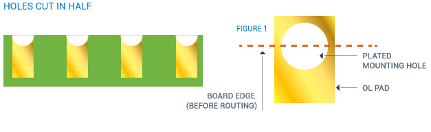
Castellations are plated through holes or vias located in the edges of a printed circuit board. Castellations are cut through to form a series of half holes. These half holes serve as pads intended to create a link between the module board and the board that it will be soldered onto.
Castellated holes can be used for a couple of different reasons. Most commonly, they are used by designers to create PCB modules, such as Wi-Fi or Bluetooth modules, which will then be used as an independent part to be placed onto another board during the PCB assembly process. However, castellations are also used when combining two boards to ensure the solder inspection joint is properly structured and to create wireless PCB to PCB links.
Yes, several. They include:
1. Half Holes.
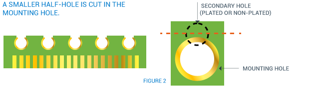
2. Holes with smaller half holes.
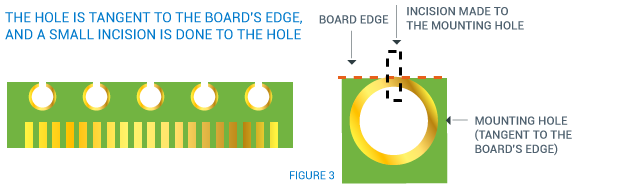
3. Holes tangent to the board's edge.
Depending on the need and final use of the board there are some design attributes that need to be met. For example:
· Size: It is recommended to use the largest possible size.
· Surface finish: Depends on the final use of the board, but ENIG is recommended.
· OL pad design: It is recommended to use the largest possible OL pad on top and bottom.
· Number of holes: This depends on the design; however, it is known that the less number of holes, the more difficult the PCB Assembly process will be.