CALL US
(800) 348-9250

EMAIL US AT
support@pcbunlimited.com
Important: All work surfaces should be conductive and grounded.
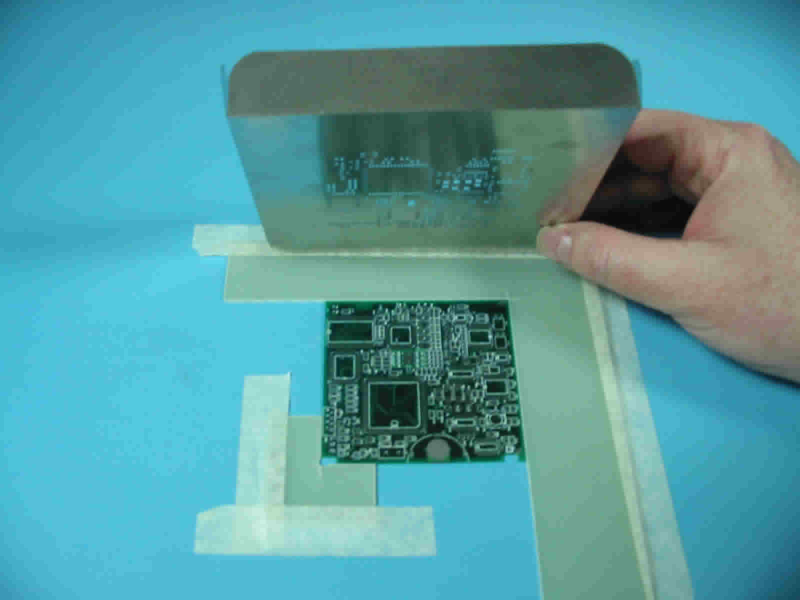
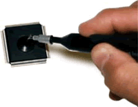
Prototype Stencil: The prototype stencil is a stainless steel foil (5 to 10 mils thick) with openings cut though to allow the solder paste to be deposited on to the PCB lands (Pads). To prevent the PCB from moving you can tape it down or you can make a smaller square and use it as indicated.
Remember: If using refrigerated solder paste, be sure to remove it from refrigeration and let it warm to room temperature. Before printing with solder paste provided in a jar, stir it for five minutes. Do NOT store paste that is not delivered in a cold pack in a refrigerator.
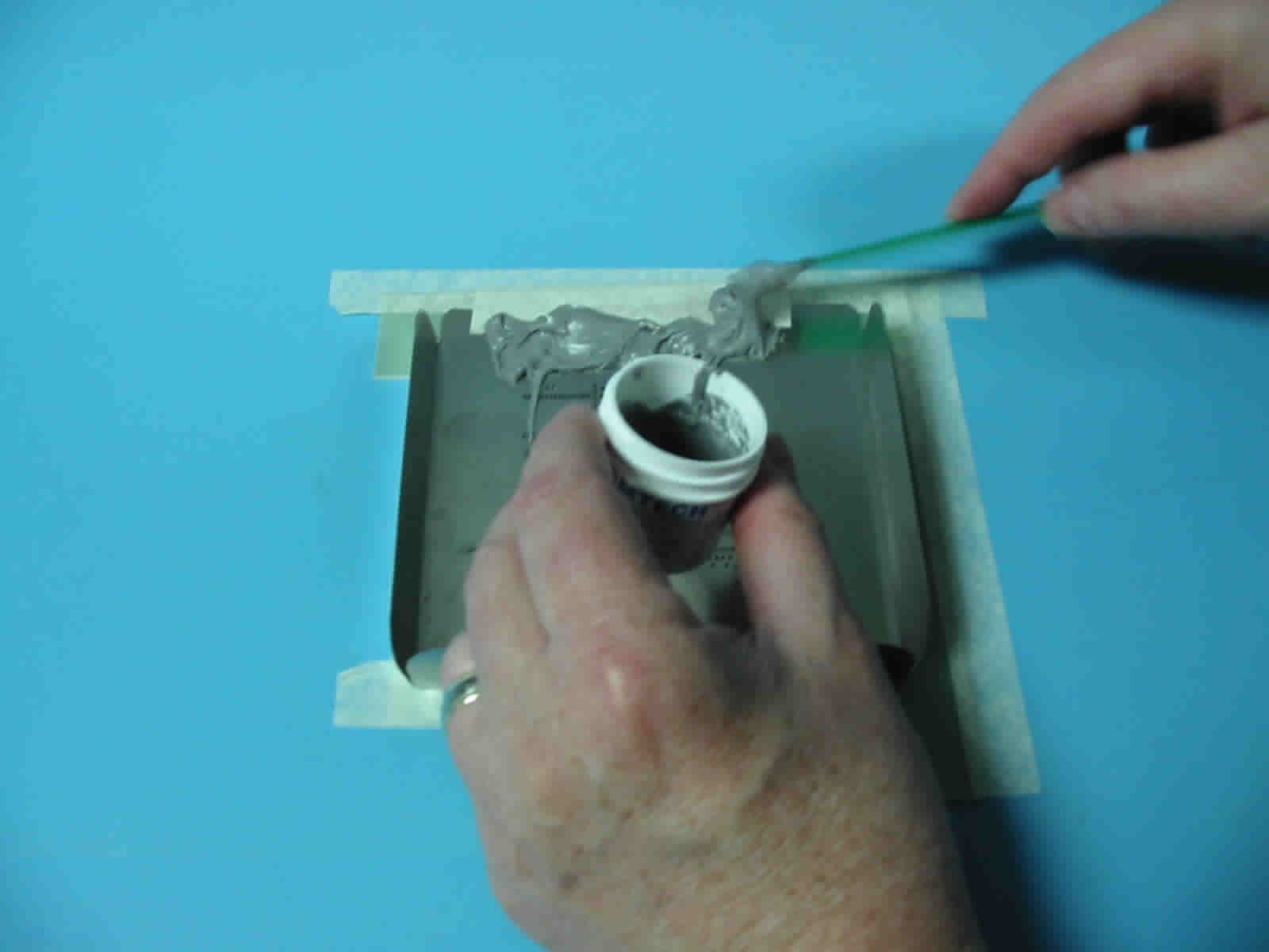
Place the solder paste on the prototype stencil to one side of the hole pattern. Spread the solder paste the full width of the hole pattern.
Squeegee: The squeegee is a flexible blade of stainless steel use to roll the solder paste over the prototype stencil forcing the solder paste thought the prototype stencil and on to the PCB lands.
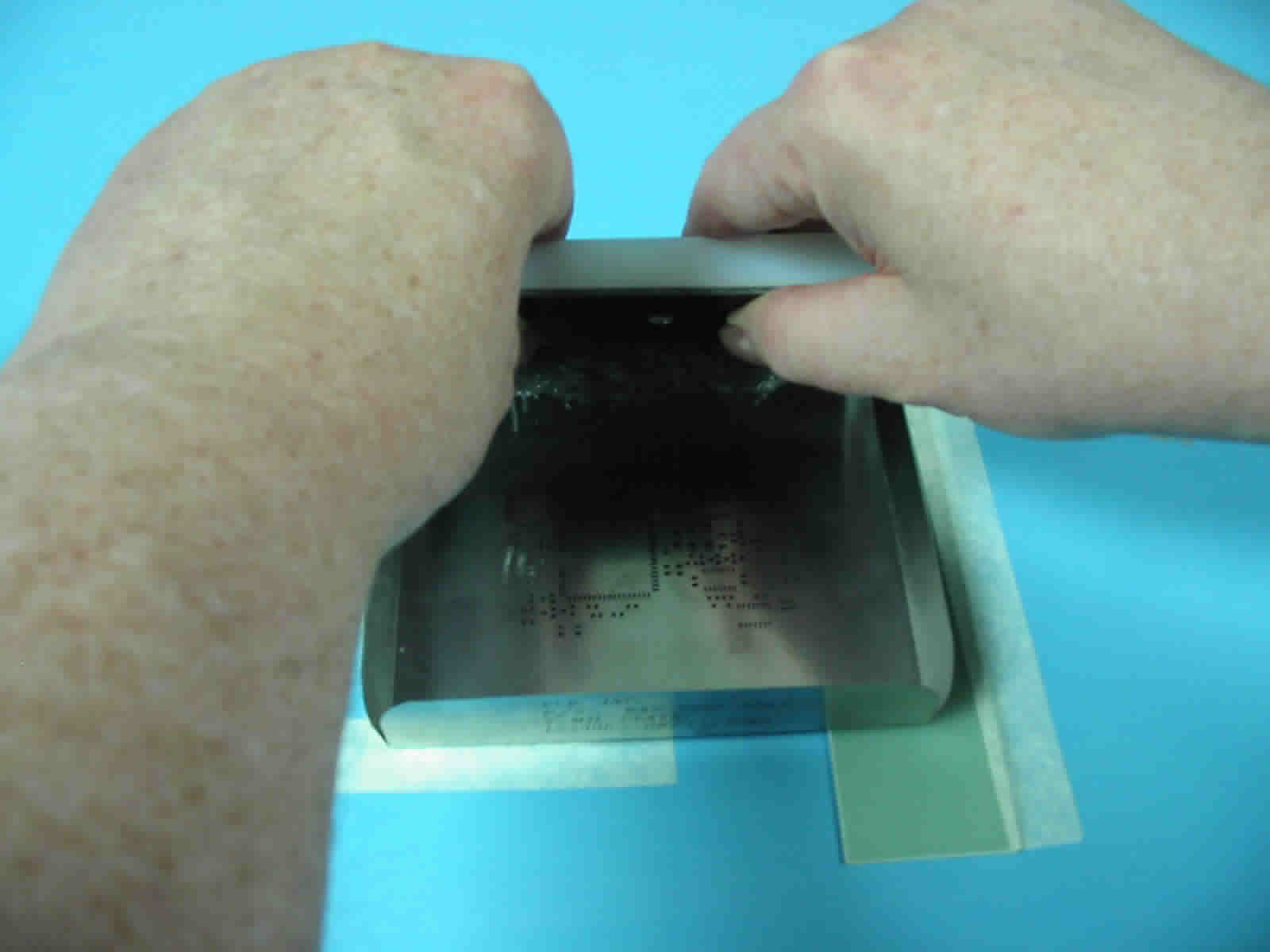
While holding the prototype stencil in contact with the PCB take the squeegee and place it on the prototype stencil outside the solder paste. *Tilt it 15 to 20 degrees from the vertical (toward the solder paste) and drag it and the solder paste across the hole pattern. Hold a light to medium pressure on the squeegee against the prototype stencil. Carefully lift the prototype stencil away (UP) from the PCB. *You may have to experiment a little to find the best angle for the type of solder paste you're using.
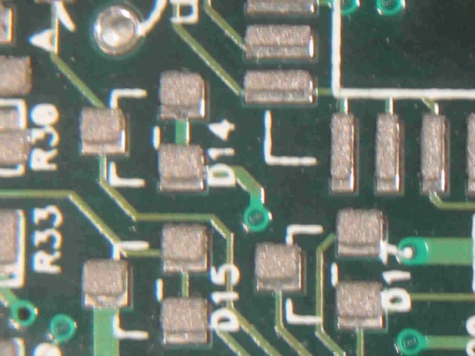
Inspect the solder paste print to ensure all the lands have solder paste on then and the paste is not smeared. If the print is not good, immediately use a spatula to remove the solder paste from the PCB. Clean the paste that remains on the PCB with alcohol and a clean rag. Let the PCB dry and print the solder paste again.
Important: Keep the time between printing the solder paste and placing the SMT parts on the solder paste short. The paste manufacturer can guide you on the maximum time between printing and placement.
Place the SMT parts on the PCB using tweezers or hand-held vacuum placement tool. (use a magnifying glass, if needed to align fine pitch leads to the land pattern.)
There are two reasons to use a temperature indicator: First, to create good solder joints solder paste has to reflow or melt at a certain temperature and stay at that temperature (liquidous) for a given amount of time. When you buy your paste, this information is provided by the solder vendor. Next, your SMDs are temperature sensitive, so you want to know how long they can be exposed to the reflow or melt temperature without damage. A temperature indicator is designed to tell you this by the way it reacts within the oven.
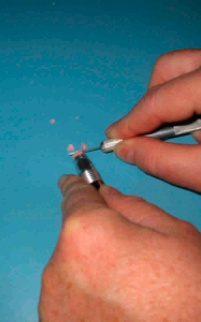
There are several types but the one that I use looks like a big crayon. I use this to make a mark on the board.
Some of these are hard to mark with, so I often just shave off a tiny bit of flakes onto the board with a knife tip. You might want to slice a small piece off. Either way works fine. It melts at the specified temperature.
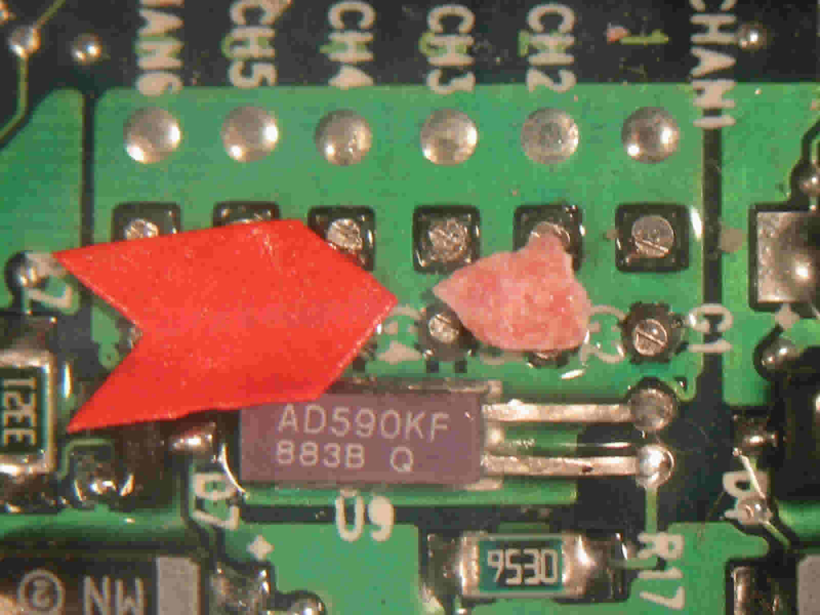
Different temperature indicators have different colors. For this process the indicators marks are light in color. They look a little like dust on the board - a little like flakes of talcum powder. When they melt they slump and change color. This particular one goes from light pink in color to clear red, so it's easy to see. Obviously, it has to be near the window of the toaster oven where you can readily see the change.
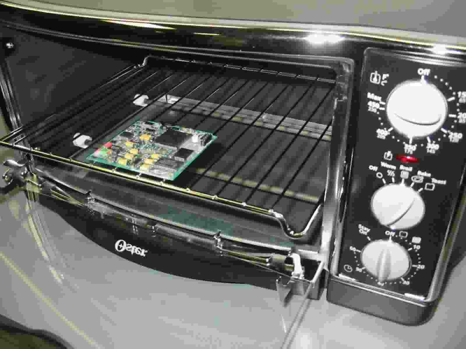
Important: Before reflowing starts, turn the oven on to heat up, a minimum of five minutes. Set the oven to bake and set the temperature to the highest baking temperature setting (450 to 500 degrees F).
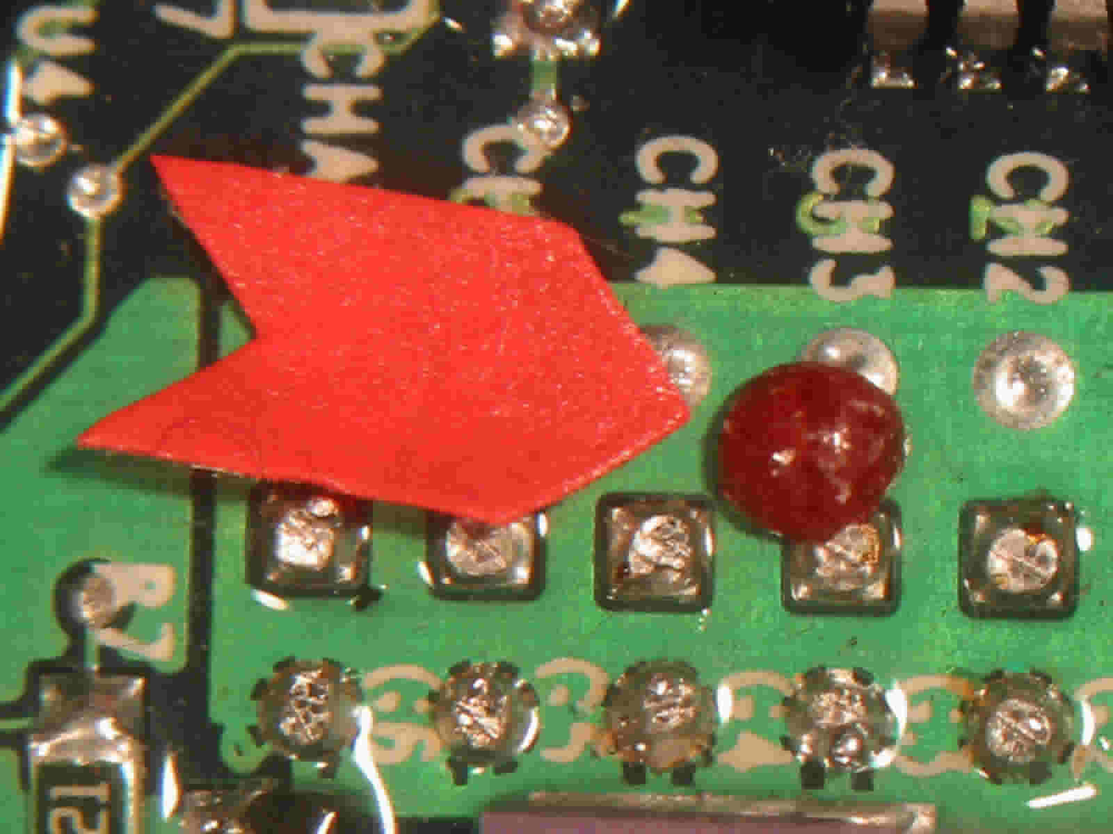
Before placing the PCB in the oven, mark it on the top side next to the edge that will be nearest to the oven door, with the reflow temperature indicator (413 degrees F).
Make sure that you can see the temperature stick mark through the oven door. If the edge of the board has a breakaway do not mark the breakaway, mark the edge of the PCB. If there is not a clear area on the edge of the PCB, mark the interior of the PCB next to a large component (PLCC or QFP) with the reflow temperature indicator.
NOTE: The edges and corners of the PCB will be hotter than the interior of the PCB. If the temperature marker is used on the interior of the PCB, the corners and edges may get too hot and damage the board or the SMT components.
When the temperature indication mark melts, remove the board from the oven. Be careful not to disturb the molten solder joints. Place the board on a surface and let it cool to near room temperature. Inspect the solder joints. Use your solder joint inspection criteria or the IPC 610 requirements.
If you have more than one board, place the next PCB in the oven after marking the board with the temperature stick. If any of the solder joints on the first board did not reflow properly, mark the PCB next to the location that did not reflow with the temperature indicator (413 degrees F). Use this location to control the reflow length for the subsequent boards or to redo the reflow process on the original board.
A flashlight can help when watching the temperature indicator material change in form. When using a toaster oven, this visual method is the only reliable reflow guide. You have to watch the material to judge reflow time. Every board is different so time is not a good control (1 minute, 5 minutes, 20 minutes, etc.). There just isn't any "average reflow time" for these types of projects. To suggest any would only confuse the issue and could actually hurt, rather than help, your project. Remove the PCB after the temperature stick mark melts, let cool and inspect the solder joints. Repeat the above step until all your PCBs are reflowed. Turn Oven off.
Learn How to Recognize A Good Solder Joint
I'm sure that many of you are either associated with or at least aware of the
Institute for Interconnecting and Packaging Electronic Circuits (IPC). This is
the best source I can point you to regarding all the guidelines you need to
build and inspect a product worthy board assembly. The documents below are extremely
helpful, even if you're an old pro. You can order them, and much more, directly
from IPC at the address below.
2215 Sanders Road
Northbrook, Illinois 60062-6135
Tel 847 509.9700
www.ipc.org
After populating and reflowing the side with the smallest components, repeat the process on the side with the larger SMT parts. This sequence will keep the largest and heaviest parts from hanging upside down during reflow, reducing the likelihood that they would fall off. Molten solder has very high surface energy and can hold most SMT parts even up side down.
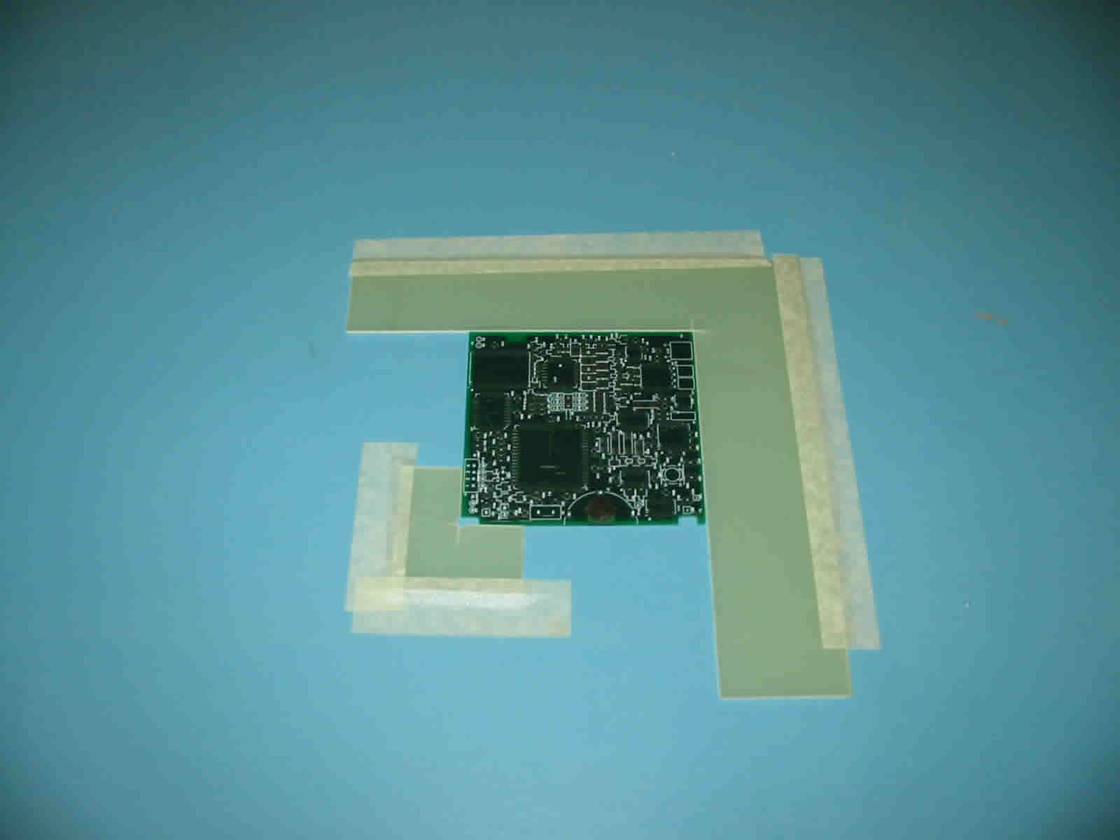
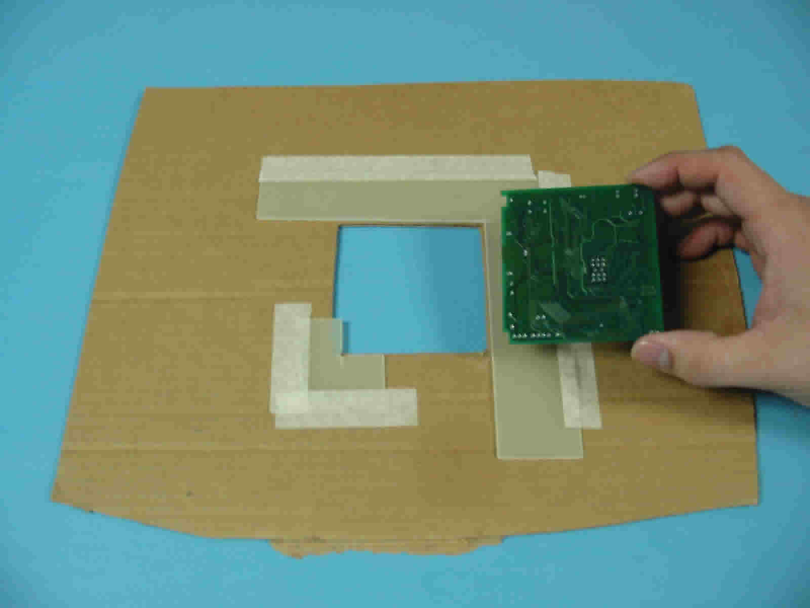
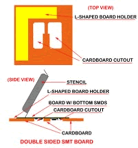
Print the second side with the PCB on cardboard* that is large enough to attach the L-shaped board holder and your board assembly. Use cardboard that is thicker than the populated PCB and thick enough to function as a support for the screening process. *Cardboard is the easiest, but you can use wood or any non-static generator.
The cardboard should be cut out to clear the SMT components from the first reflow. Again, make sure all work surfaces are ESD safe or grounded.
Tape the cardboard "holder" to the work table and do everything on top of the cardboard the same as you did when screening solder paste on the first side. The reflowed components nest safely in the openings in the cardboard. The board rests flat on the cardboard with the surface to be screened is open to the prototype stencil.
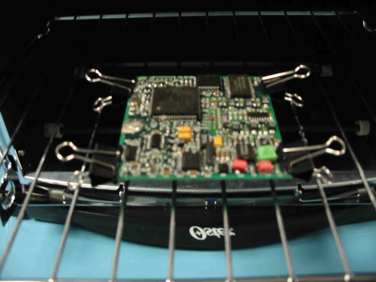
When you reflow the second side of the PCB, the whole assembly has to be held off the oven shelf with standoffs. You'll damage the SMT solder joints from the first reflow if you lay the board directly on the oven shelf.
You can use any material that can withstand the oven temperature to create stand offs to hold the board, but the very best is scrap FR4 material. You probably have some old board scraps laying around, but if not, just prop the assembly up on a couple of pieces of metal or anything that is not going to be affected by the heat of the oven. I used large binder clips for this board and they worked fine.
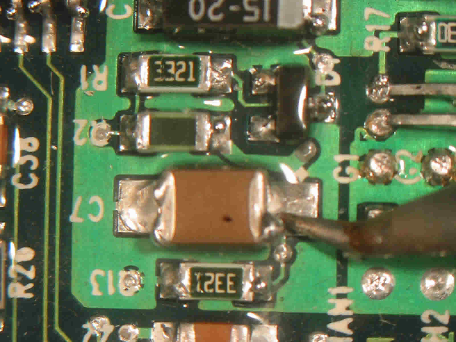
Touch up any solder defects with a solder iron. Use a fine tip on the solder iron and don't let the tip touch the body of the SMT parts. Set your solder iron temperature as low as possible. A solder iron that is set to a high temperature can thermal shock SMT components.
That's it. You now have your finished boards, ready to test and use in your latest project. Make sure you handle your SMT and mixed technology SMD board(s) carefully. They're not as rugged as 100% through hole, but what you can create with them is far beyond anything you could ever get with only through hole. Experiment. Have fun.
Questions? Contact us and I'll do the best to help.
support@pcbunlimited.com
Phone: (800) 348 9250