
CALL US
(800) 348-9250

EMAIL US AT
support@pcbunlimited.com
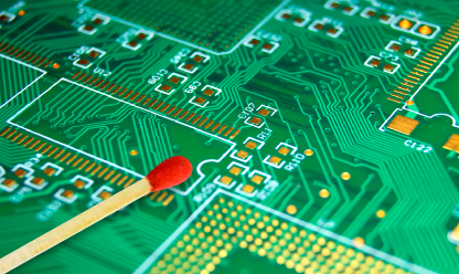
There are many of types of PCBs to choose from when doing prototyping, ranging from simple one-sided PCBs to incredibly complex, multi-layer boards. Generally, the most simple prototype printed circuit boards are the ones that contain copper tracks, or interconnections between its components on only one of its surfaces. These boards are known as one-layer printed circuit boards, or single sided PCBs.
However, in the manufacture of more complicated circuit boards, there is a need for HDI PCBs. Known as High Density Interconnect, these printed circuit boards have a higher wiring density than traditional PCBs. Along with thinner spaces, smaller vias, and a higher connection pad density, these boards boast a lot of different advantages to the typical prototype circuit boards.
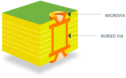
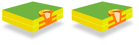
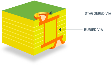
One of the main features of HDI PCBs, is that they not only use Vias to create connections between layers, this type of circuits also uses Laser Drilled Microvias, which are smaller and more effective in terms of space. There are at least 5 different types of Via/Microvias arrengements that can be used in HDI PCBs:
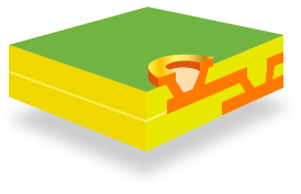
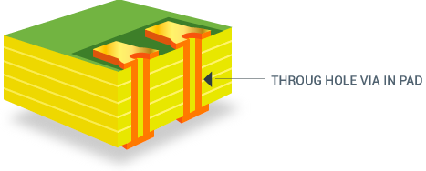
Utilizing any of these HDI PCBs schemes will benefit any project that requires complex wiring but also faces size restraints.
Some benefits of these specific printed circuit boards include:
· These PCBs are extremely compact. Considering that HDI PCBs have a higher wiring capacity, they are one of the best options for engineers looking for the smallest circuit board with the largest output. HDI capacity makes it easier to turn a 10 layered PCB into a four or five layered one, which is great for those looking for smaller boards without skimping on quality. Since most consumers prefer small devices, this can be a huge design advantage.
· The ability to place more components on one side. These HDI PCBs utilize blind and buried vias, and Via-in-Pad technology, as methods of placing components closer together, which results in faster signal transmission. Making it an ideal technology for RF circuits.
· Laser drill technology makes PCBs into advanced electronic circuits. This manufacturing technique allows for smaller holes to be used and gives the board higher heat resistance.
Using High Density Interconnect PCBs will elevate your technology to a whole new standard. These small PCBs are cost effective, withstand higher frequencies, and are great when used in mobile devices, such as laptops, cell phones, and tablets. Of course, this is just a brief introduction to this technology, which is fast becoming a go-to option for electrical engineers. Need more advanced information? Then please do not hesitate to contact our professionals today to learn more about this interesting form of PCB technology.