 Not to be confused with printed electronics, prototype printed circuit boards connect electronic components using conductive tracks. They can be extremely versatile, but in order to incorporate them into your designs you’ll need to be grounded in the basics. To get started, here is everything a beginner must know about prototype PCBs.
What are they used for?
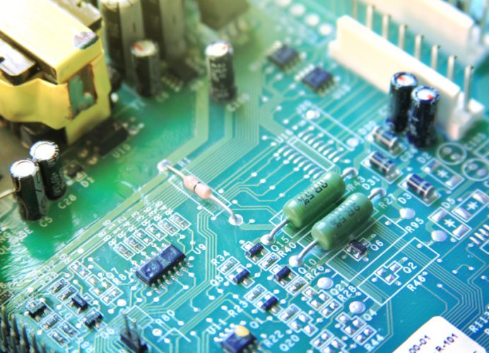
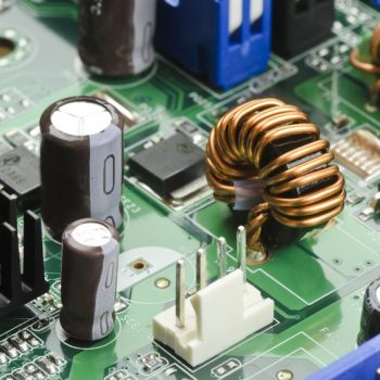
As they route signals and power through electronic devices, they provide mechanical and electrical connections in many everyday objects. This includes computers, electronic toys, flashlights, e-readers, you name it.
What is the structure of a circuit board?
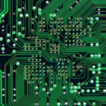
The most simple printed circuit boards are one sided and have copper tracks that interconnect on only one surface. These are known as 1 layer PCBs. But you can also find double-sided and multi-layered PCBs that have conductive paths on all sides. If you’re having trouble forming a mental image, picture lasagna.
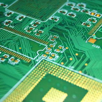
The compositions of prototype printed circuit boards are similar to lasagna in that there can be many layers. Simply put, from the bottom up there is substrate (FR4), copper, soldermask, with silkscreen at the top.
FR4: this base material is usually made out of fiberglass. It is what gives the PCB its rigidity and thickness.
Copper: this is laminated to the board using heat and an adhesive. It’s the basis for double-sided and multi-layered boards, which are determined via the number of copper plates used. It is specified by weight, and generally PCB designers use one or two ounces of copper per board.
Soldermask: this layer insulates the copper traces from coming in contact with other metal while also preventing solder jumpers.
Silkscreen: as the final layer, the silkscreen adds numbers and letters to the PCB to allow better assembly. Any ink color can be used, but white is a popular choice.
How are prototype circuit boards manufactured?
There are two kinds of construction processes to fabricate prototype printed circuit boards, through-hole and surface mount technologies.
What is through-hole technology?
This method mounts electronic circuits by leads inserted into the holes on one side of the board, and soldered to the copper layer on the other side.
What is surface mount technology?
This newer method allows for the components to be soldered directly onto the surface of the board, instead of having to use leads. This allows for the fabrication of much smaller PCBs with higher circuit densities.


Related Posts
Manufacturing Techniques of Printed Prototype Circuit Boards
While prototype circuit boards are used in everything from cell phones to computer monitors, to…
Tips and Tricks for an Efficient PCB Layout
When building prototype circuit boards, engineers typically focus the majority of their attention on formatting…
Scottish and Chinese Researchers Discover New Ways to Recycle Prototype Circuit Boards
Prototype printed circuit boards are necessary components in anything electronic, from old computers to mobile…